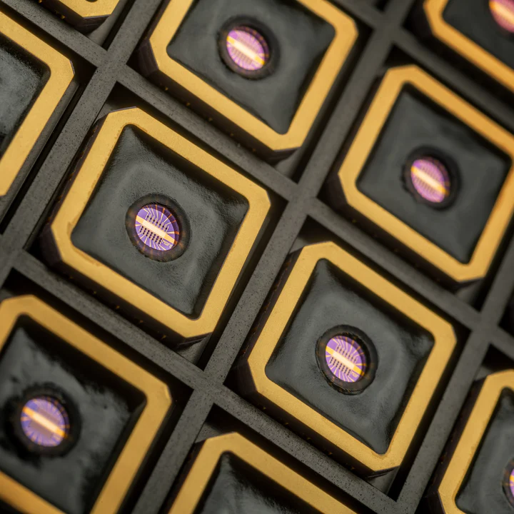
[Graphena] mGFET-4D for Sensing applications

TYPICAL SPECIFICATIONS
- · Growth method: CVD synthesis
- · Polymer assisted transfer
- · Die dimensions: 4 mm x 4 mm
- · Chip thickness: 525 μm
- · Number of channels per chip: 28
- · Gate Oxide thickness: 90 nm
- · Gate Oxide material: SiO2
- · Resistivity of substrate: 1-10 Ω·cm
- · Metallization: Au contacts
- · Encapsulation: 50 nm Al2O3
- · Graphene field-effect mobility: >1000 cm2/V.s
- · Dirac point (liquid gating in PBS): <1 V
- · Yield: >75 %
APPLICATIONS
Graphene field-effect transistors (GFETs) have unprecedented sensitivity to the surrounding environment and is an ideal transducer for a variety of sensing applications. Depending on the application, mGFETs can be tuned to be sensitive only to the stimulus of interest and have shown breakthrough performance in areas such as graphene device research, chemical/gas sensing, biosensors, chemical sensors, Bioelectronics, healthcare and industrial safety applications.
mGFET-4D (4 mm x 4 mm) - Processed in Clean Room Class 1000
The mGFET 4x4 chip from Graphenea is designed for sensing applications, and it is compatible with measurements in a liquid medium. The metal pads are passivated to avoid degradation and reduce leakage currents. It also includes a non-encapsulated electrode at the center of the chip, which allows for liquid gating without the need of an external gate electrode (such as Ag/AgCl probes). This device architecture enhances signal-to-noise ratio and reduces parasitics.
This version provides 28 graphene graphene channels: 7 of them are one-channel devices and 7 of them are three-channel devices. These two geometries add flexibility to the measurement scheme (ΔVD or ΔIsd). The die is packaged and wirebonded to a leadless chip carrier (LCC) and it is fully compatible with the Graphenea Card
'Graphenea' 카테고리의 다른 글
| [Graphenea] Graphenea Card (0) | 2025.05.02 |
|---|---|
| [Graphenea] mGFET-4P for Sensing applications (0) | 2024.02.15 |
| [Graphenea] mGFET-4P for Sensing applications (0) | 2022.07.14 |
| [Graphenea] Monolayer Graphene on 90 nm SiO₂/Si (0) | 2021.09.10 |
| [Graphenea] Easy Transfer: Monolayer Graphene on Polymer Film (0) | 2021.08.24 |


